Privacy statement: Your privacy is very important to Us. Our company promises not to disclose your personal information to any external company with out your explicit permission.
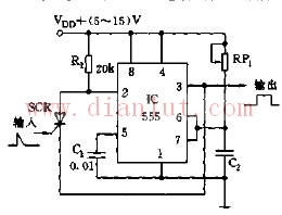
As shown in the figure, 555 and R1, RP1, C2, etc. constitute a trigger delay circuit. Normally, since R1 is connected to VDD, 555 is in the reset state, that is, the 3 pin is at a low level; when the trigger signal arrives, the SCR is turned on, and the 2 pin has a low level signal, so that the 555 is inverted and the output is high. The temporary stability width is τ=1.1RP1C2. After triggering, the SCR is turned off. This circuit reduces the need for trigger pulses. If the CMOS type 555 (or 556) is used, the trigger current can also be reduced.

August 12, 2024
The full name thyratron, commonly known as thyristor, is a bistable power electronic device that contains 3 or more PN junctions that can switch from off-state to on-state or from on-state to...
When the thyristor damage need to check the analysis of the reasons, the core can be removed from the cooling jacket, open the core box and then remove the chip, observe the signs of damage to...
A special sealing device is made by the method of disposing the dust in the radiator. This kind of device only leaves the fan through hole. Go to the construction site and construction site to...
In order to prevent damage to the thyristor caused by the failure of the AC circuit inversion of the thyristor, the traditional method is to use a fast fuse for overcurrent protection. The advantage...
Email to this supplier
August 12, 2024
August 14, 2023
January 07, 2021

Privacy statement: Your privacy is very important to Us. Our company promises not to disclose your personal information to any external company with out your explicit permission.

Fill in more information so that we can get in touch with you faster
Privacy statement: Your privacy is very important to Us. Our company promises not to disclose your personal information to any external company with out your explicit permission.